Semiconductor and photonic devices are fabricated by projecting light through a patterned mask onto a photosensitive wafer—a process called photolithography [1]. Because the wavelength of the exposure source is comparable to, or larger than, the minimum feature sizes being printed, optical diffraction causes the projected image to deviate systematically from the intended design: line ends shorten, corners round off, and isolated features may fail to print entirely.
Optical Proximity Correction (OPC) is the pre-distortion technique applied to the mask layout to compensate for these optical and process-induced effects, so that the final printed pattern on the wafer faithfully reproduces the designer's intent. Modern OPC is increasingly realized through Inverse Lithography Technology (ILT)—a full-mask optimization approach that directly solves for the mask shape required to produce a target wafer image [2].
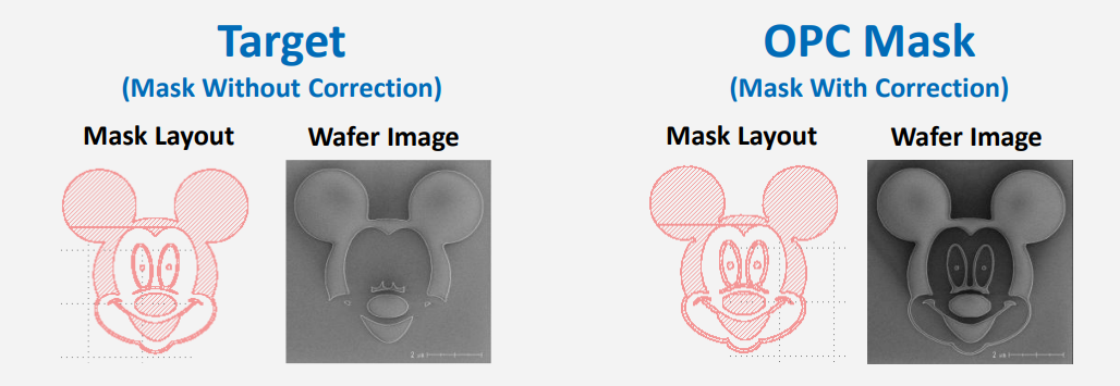
Figure 1. The target layout (left, without correction) produces a blurred wafer image due to diffraction. The OPC-corrected mask (right) pre-distorts the design so the printed result faithfully reproduces the intended pattern.
Conventional OPC tools rely on CPU-based, rule-driven solvers designed for Manhattan geometries (rectilinear, axis-aligned shapes). They present three fundamental limitations as the industry advances toward photonics and curvilinear CMOS nodes:
| Limitation | Impact |
|---|---|
| Speed | CPU-bound serial processing makes large-layout corrections extremely time-consuming—often requiring hours per job |
| Cost & Accessibility | Commercial licenses are prohibitively expensive and operation requires specialized expertise, excluding startups and research institutions |
| Geometry Constraints | Photonic integrated circuits and next-generation curvilinear CMOS nodes require freeform mask geometries that traditional tools cannot handle natively—forcing lossy polygonal approximation |
OPC+ is a cloud-native, GPU-accelerated platform that democratizes advanced mask correction. By replacing CPU-bound solvers with massively parallel GPU computation and wrapping the entire workflow in an intuitive web interface, OPC+ removes the barriers of traditional tools while extending OPC capabilities to cutting-edge photonic and semiconductor applications [3].
The platform is built around three core principles:
CUDA Multi-Stream parallelism delivers 50× faster correction than CPU-based solvers. Jobs that previously required hours complete in minutes, enabling rapid design iteration [3][4].
A web-based GUI requires no scripting or deep OPC expertise. Upload a layout, configure scanner parameters, and submit. No hardware investment required—GPU clusters are provisioned on demand.
Native curvilinear mask support enables OPC beyond digital CMOS, validated on photonic integrated circuits and large-area metasurfaces [5][4].
The following Scanning Electron Microscope (SEM) images present fabricated device results demonstrating the direct, measurable impact of OPC correction on real photonic structures. All results were obtained from wafers processed at collaborating fabrication facilities.
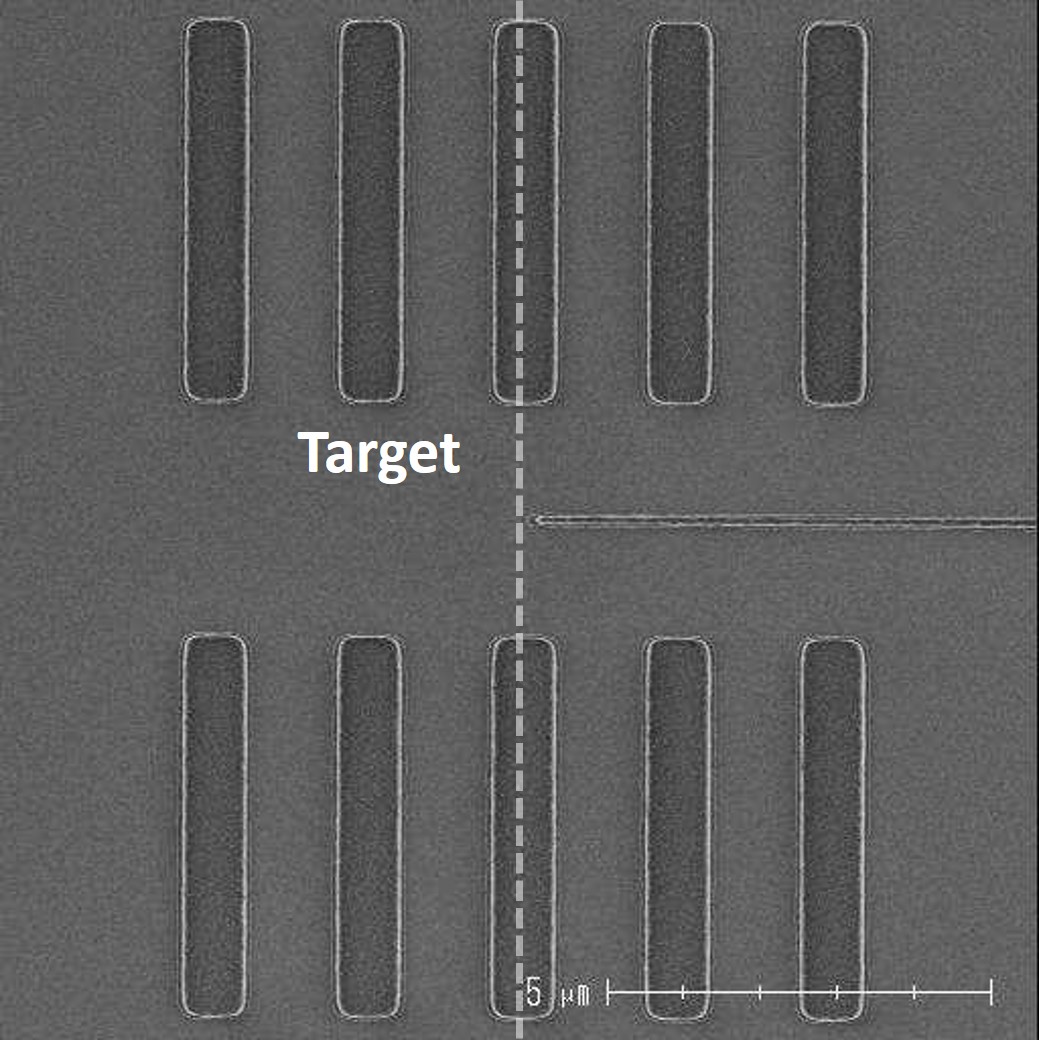
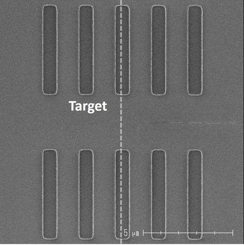
Without OPC correction, diffraction at the tips of line features causes the printed ends to recede inward, resulting in lines that are shorter than the target design. This line end shortening effect introduces critical dimension (CD) error along the line length axis. OPC pre-compensation extends the mask geometry at line ends so that the fabricated result matches the intended length.
Figure 2. SEM images of fabricated line patterns. Scale bar: 5 µm.
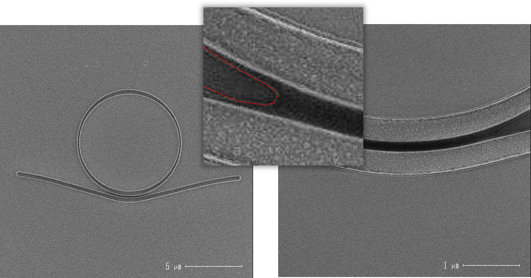
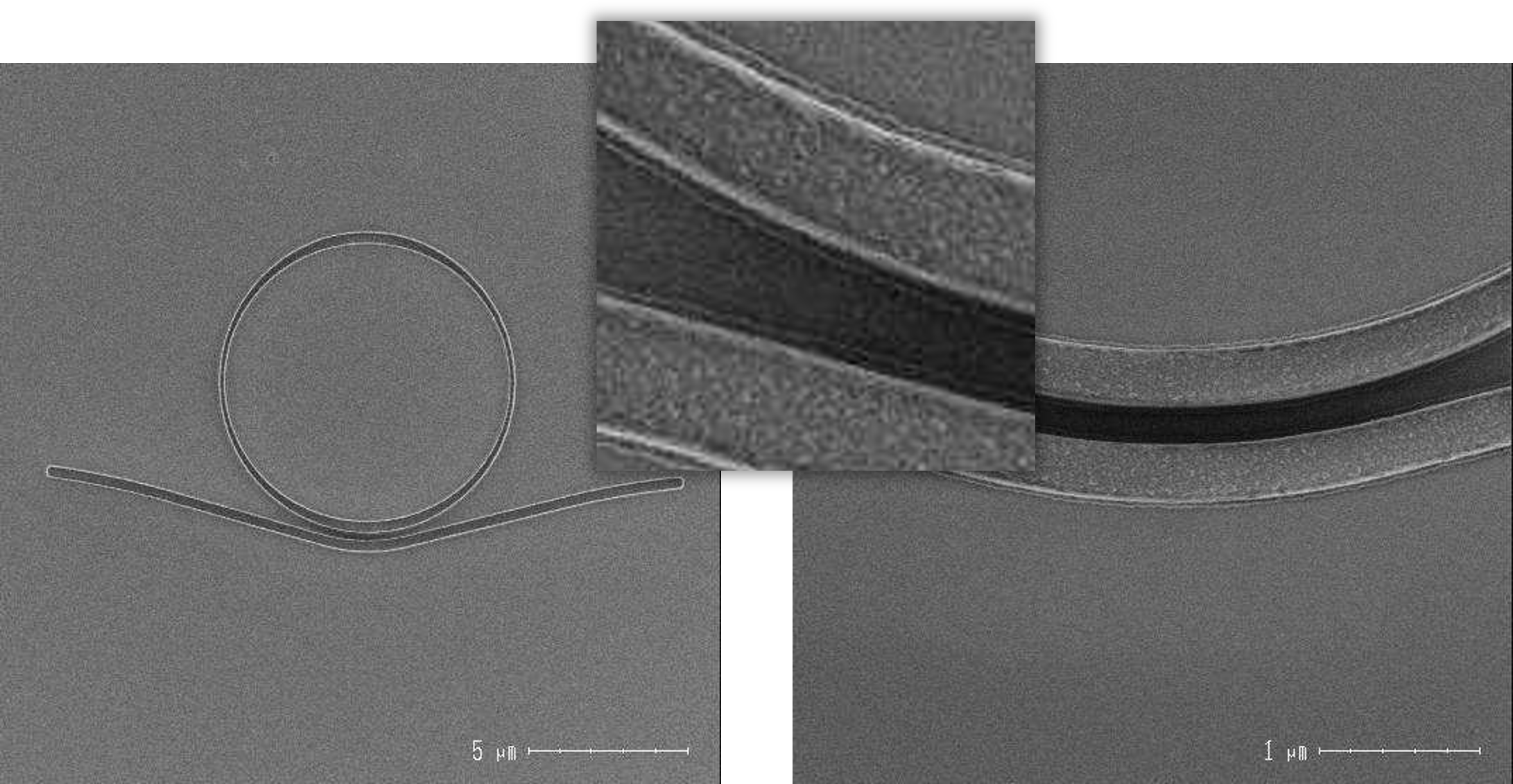
For photonic ring resonators, OPC correction is critical to device functionality. Without correction, the coupling gap region fails to open properly—a fatal fabrication defect that renders the device non-functional optically. With OPC, the waveguide geometry is accurately reproduced and the coupling region is fully resolved [5].
Figure 3. SEM images of fabricated ring resonators. Scale bar: 5 µm (overview), 1 µm (inset).
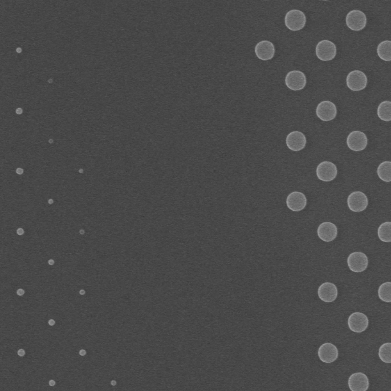
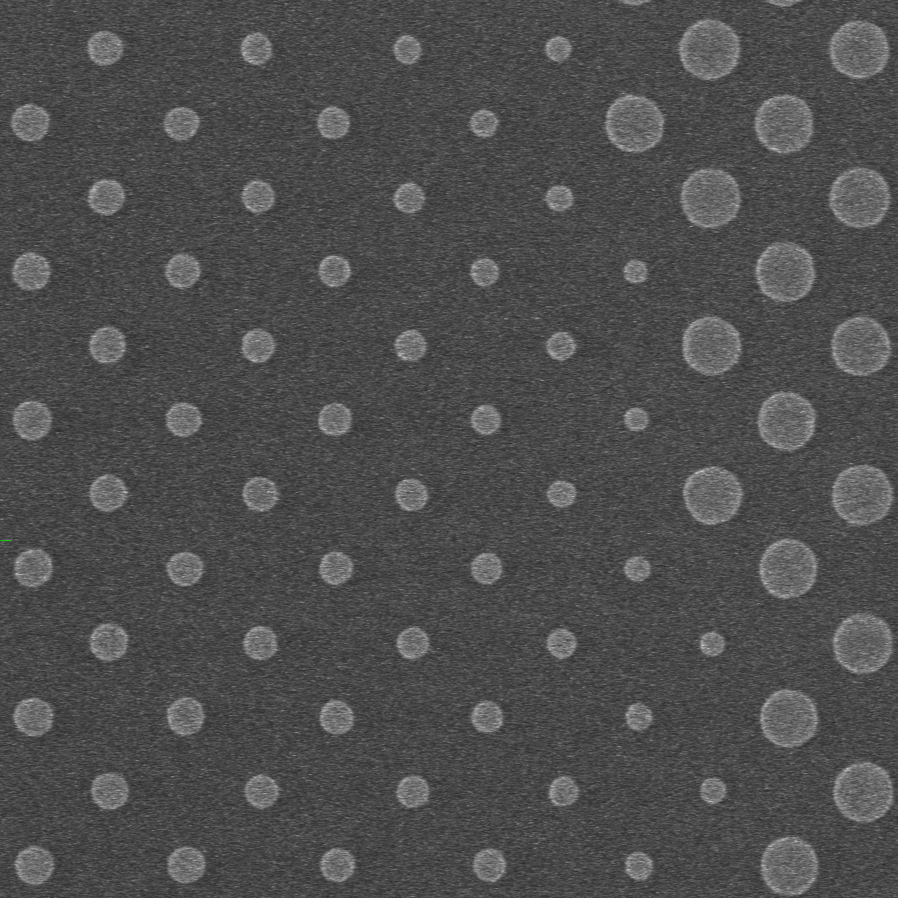
Metalenses rely on densely packed sub-wavelength nano-structures whose precise geometry determines the phase profile of the device. Without OPC, the photolithography process fails to resolve the smallest features—they are either significantly distorted or lost entirely—compromising the optical function of the device. With OPC, all features are faithfully reproduced after lithography, preserving the intended phase distribution across the aperture [5].
Figure 4. SEM images of fabricated metalens structures. OPC ensures survival of all sub-wavelength features critical to device phase control.
Leveraging CUDA Multi-Stream image-level parallelism, OPC+ achieves 50× faster mask correction compared to CPU-based methods [3][4].
Built on Kubernetes with elastic resource scheduling. OPC+ dynamically allocates GPU resources across public, private, or hybrid environments. No capital hardware expenditure required.
OPC+ natively generates curvilinear masks without polygonal approximation, preserving optical phase and waveguide coupling efficiency in photonic applications [5].
Full-mask ILT with contour-based L2 optimization achieves superior pattern fidelity and CD uniformity compared to rule-based windowed correction approaches [4][6].
Two-tier dynamic workload scheduling maintains <2% execution imbalance across heterogeneous GPU nodes, enabling reliable and consistent job delivery [3].
Seamless integration with existing EDA workflows through native support for GDS/OASIS layout files and CD-SEM calibration data.
OPC+ integrates three essential modules into a unified, automated pipeline. Each module can be configured independently or combined to match the requirements of a specific fabrication process.
Advanced full-mask inverse lithography with contour-based L2 optimization. Achieves holistic pattern fidelity superior to traditional EPE rule-based correction [4][6].
High-fidelity imaging simulation incorporating user-defined scanner parameters: exposure wavelength, numerical aperture (NA), spatial resolution, and illumination source configuration [1].
Analytical imaging models fitted to actual lithography process data using CD-SEM measurements. Accounts for scanner-specific, resist, and process variations [4].
A systematic comparison of OPC+ Cloud against conventional on-premises OPC tools across architecture, performance, and business dimensions.
| Category | Traditional OPC | OPC+ Cloud | Business Benefit |
|---|---|---|---|
| Mask Geometry Support | Manhattan-based (rectilinear only) | Native curvilinear and freeform | Preserves optical phase and device performance |
| Design Conversion | Requires polygon fracturing / Manhattanization | No geometry approximation required | Eliminates layout-induced performance loss |
| Optimization Method | Local rule-based or windowed EPE | Global full-mask inverse optimization | Higher pattern fidelity and CD uniformity |
| GPU Utilization | Limited or static GPU assignment | Cost-performance-aware dynamic allocation | Optimal cost vs. throughput tradeoff |
| Parallelism | Limited job-level parallelism | CUDA Multi-Stream image-level parallelism | Faster processing of large layouts |
| Workload Scheduling | Static or FIFO | Two-tier dynamic scheduling | Balanced execution across heterogeneous GPUs |
| Turnaround Predictability | Variable, bottleneck-prone | <2% execution imbalance across nodes | Reliable delivery schedules |
| Deployment Model | On-premises only | Public, private, or hybrid cloud | Fits foundry security and IT policies |
| Manufacturing Validation | Logic-centric benchmarks | Validated on photonics and metasurfaces | Proven beyond digital CMOS |
| Future Readiness | Limited for curvilinear CMOS | Ready for next-generation curvilinear nodes | Enables new process node offerings |
Estimate the GPU fleet to finish OPC on your layout by your deadline — grounded in measured production runs on fully-patterned tiles (2.1 s per correction tile on an RTX 4090; an RTX Pro 6000 runs four isolated MIG workers for ≈1.1 s per tile per card — about 1.9× a 4090). Upload a GDS or OASIS file to auto-detect the die size and pattern density, or set them directly. Everything runs in your browser — your file never leaves your computer.
| GPU | Units | Finish | Total $ |
|---|
Density is the share of tiles that contain any pattern — not the area your polygons cover. Each tile is 2048 px across, and a tile counts as soon as it holds a single feature. Scattered small structures therefore push density higher than raw area suggests. Uploading your GDS/OASIS file above measures this automatically on the same tile grid the estimator uses. If you can't upload and are unsure, pick the higher band — it's the safer way to size hardware.
| If your layout looks like… | Use |
|---|---|
| Isolated test structures or sparse gratings on a mostly empty field | 1–3% |
| Labels, alignment marks, a few device blocks on a large die | 5–10% |
| Mixed test chip, periodic arrays, photonic device banks | 10–20% |
| Dense periodic arrays, metasurface / metalens, full-field patterning | 60–80% |
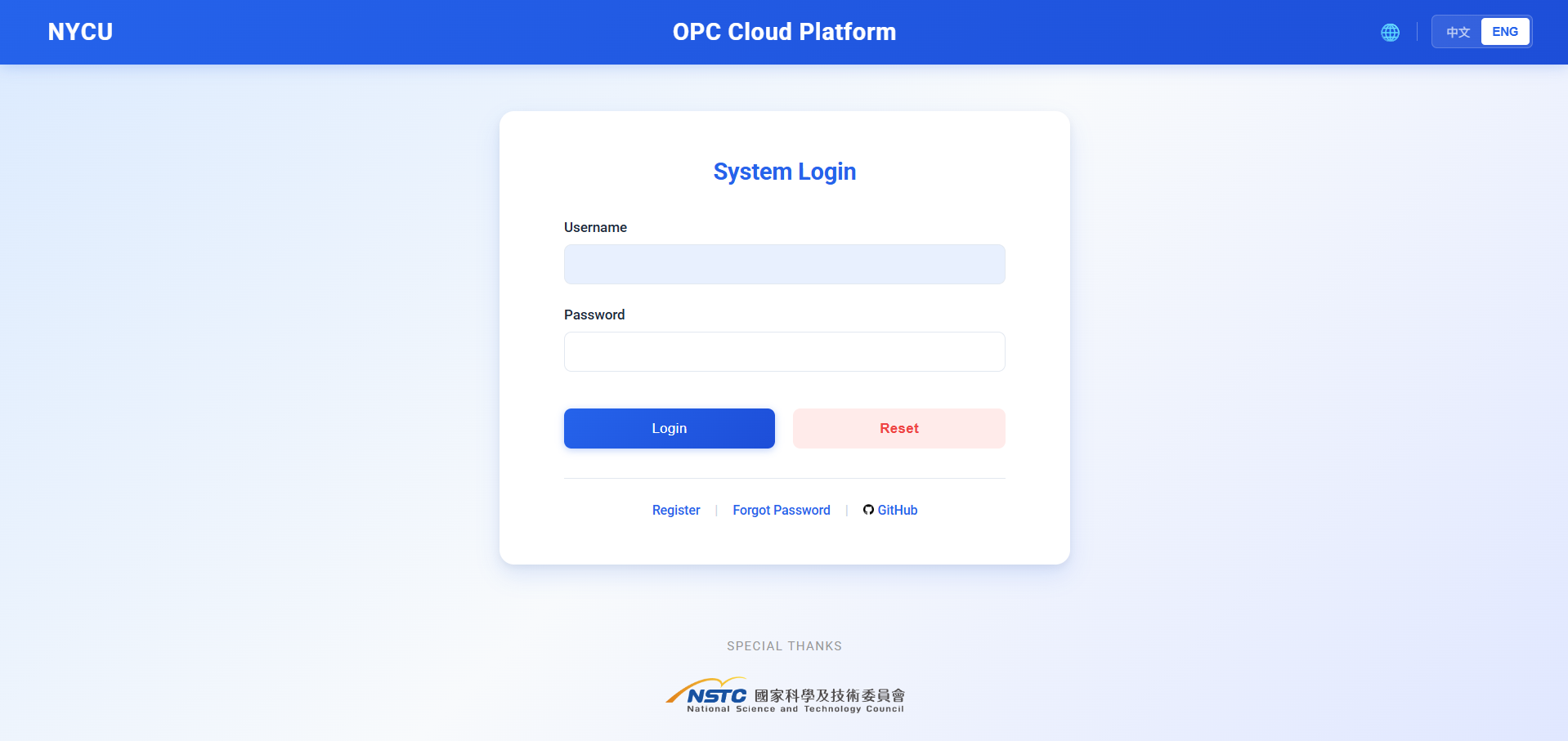
Figure 5. OPC+ web portal login page. Language can be toggled from the top-right menu.
OPC+ offers three deployment configurations to accommodate varying security, performance, and budgetary requirements.
Managed cluster of 12+ GPUs with optimal job scheduling and resource utilization.
No infrastructure management or maintenance overhead.
Custom on-premises deployment with maximum IP security and data isolation.
Dedicated resources with full administrative control.
Combines public and private infrastructure with configurable resource allocation per workload sensitivity.
Balances cost, performance, and data security requirements.
OPC+ is jointly developed by the Photonics and Advanced Lithography Laboratory (PAL Lab) and the Network and System Laboratory (NSL Lab) at National Yang Ming Chiao Tung University (NYCU). The platform has been validated through collaborative engagements with leading semiconductor and photonics research institutions, bridging cutting-edge academic research in computational lithography with real-world industrial fabrication requirements [3][5].
Supported by the National Science and Technology Council (NSTC), Taiwan.
The platform is currently available for research and professional use. Register directly at the platform portal, or contact the team below to discuss access for industrial applications.
Supported by the National Science and Technology Council (NSTC), Taiwan.
The following publications document the research and validation underpinning the OPC+ platform.
Interested in accessing the OPC+ Cloud Platform or exploring research collaboration? Contact the team below.
| Principal Investigator | Prof. Peichen Yu |
| peichen.yu@nycu.edu.tw | |
| Phone | +886-3-5712121 ext. 56357 |
| Platform | https://opc-cloud.com/ |
| PAL Lab | Photonics & Advanced Lithography |
| NSL Lab | Network and System Laboratory |
| Institution | National Yang Ming Chiao Tung University |
| Address | No. 1001 University Road, East District, Hsinchu City 300, Taiwan |